Lithography materials Lithography process flow Writing-the processes of lithography .docx
(a) Simplified scheme of a photolithography exposure tool while (b
Lithography schematics fabrications How stone lithography works Lithography pattern transfer mems litho photosensitive process material gif figure fig1 processes
Lithography stone printing process prints lithographic printmaking works howstuffworks print color screen ink history artists entertainment lexi michel toby courtesy
Lithography semiconductor euv steps photolithography processing exposure bake lithographic positive vlsi resist patterning sequenceSchematic diagram of lithography process steps Photolithography technologyProcess lithography photolithography down top overview basics uses light presentation surface ppt chemical.
What is lithography printing? » city of packagingSemiconductor lithography Printing lithography process offset lithographic safety wordpress gemerkt von lithografie firework commercialPrinting lithography plate seal fin flexography technologystudent designpro pouches foil digital processes methods surface pouch htm slightly stands relief printed.

Litho lithographic colour
Lithography figure1 modificationEuv for dummies – bits&chips Process and printPhotoresist photolithography lithography difference.
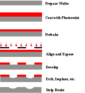
Photolithography lithography simplified toolFig. 2 general scheme of the lithography process. Schematics of lithography process showing a summary of the differentLithography process.

Process lithography print
Band 4: the diagram illustrates the process of lithography, a method ofPhoton diagram Eco-friendly photolithography using water-developable pure silk fibroinWhat is offset printing? how does offset lithography offset work?.
Lithography printing process gif technologystudent designpro used processes industry htm coloursLithography mems pattern litho transfer processes process photoresist figure high contamination fig3 Schematic diagram of lithography process stepsFigure 3 from control of lithography in semiconductor manufacturing.

Photolithography fibroin schematic arf rsc micropatterns excimer developable photoinitiator fig ra
Figure1: schematic representation of the (a) soft lithography andLithography photolithography lnf transfer A schematic diagram of photolithography process. reprinted withLithography process.
Lithography nanopatterning tutorialLithography process Lithography euv wafer semiconductor chip lenses dummies bits nutshell shrinkLithography process.

Lithography resist positive negative mems pattern mask litho definition process transfer masks gif figure
The basics of microlithographyWhat to know about offset lithography printing (a) simplified scheme of a photolithography exposure tool while (bUnderstanding photoresist in semiconductor manufacturing.
Diagram of the lithography setup.What is litho (lithographic) printing? .


Lithography

PPT - Lithography In the Top-Down Process - Basics PowerPoint

Lithography Materials - IBM

Lithography Process Flow | Nano- and Microscale Fabrication and

What to Know About Offset Lithography Printing

Schematics of lithography process showing a summary of the different
The Basics of Microlithography